
Abstract
Detailed and accurate 3D mapping of dynamic environments is essential for machines to interface with their surroundings1,2,3 and for human–machine interaction4,5. Although considerable effort has been made to create the equivalent of the complementary metal–oxide–semiconductor (CMOS) image sensor for the 3D world, scalable, high-performance, reliable solutions have proven elusive6,7,8,9,10,11. Focal plane array (FPA) sensors using frequency-modulated continuous-wave (FMCW) light detection and ranging (LiDAR) have shown potential to meet all of these requirements and also provide direct measurement of radial velocity as a fourth dimension. Previous demonstrations12,13, although promising, have not achieved the simultaneous scale and performance required by commercial applications. Here we present a large-scale, coherent LiDAR FPA enabled by comprehensive chip-scale optoelectronic integration. A 4D imaging camera is built around the FPA and used to acquire point clouds. At the core is a 352 × 176-pixel 2D FMCW LiDAR FPA comprising more than 0.6 million photonic components, all integrated on-chip together with their associated electronics. This represents a five times increase in pixel count with respect to previous demonstrations12. The pixel architecture combines the outbound and inbound optical paths within the pixel in a monostatic configuration, together with coherent detectors and electronics. Frequency-modulated light is directed sequentially to groups of pixels by in-plane thermo-optic switches with integrated electronics for driving and calibration. An integrated serial digital interface controls both optical switching and readout synchronously. Point clouds of objects ranging from 4 to 65 m with per-pixel integration time compatible with frame rates from 3 to 15 frames per second (fps) are shown. This result demonstrates the capabilities of FMCW LiDAR FPA sensors as enablers of ubiquitous, low-cost, compact coherent 4D imaging cameras.
Main
The introduction of automation into everyday life has marked a pivotal moment in our society. Across various fields, from spatial mapping for reconnaissance and construction1,2,3 to facial recognition, virtual and augmented reality4 and autonomous driving5, accurate 3D representation of dynamically evolving environments is paramount for safe human–machine interaction. Therefore, substantial research efforts are directed towards developing a cost-effective, high-performance and scalable 3D imaging sensor comparable with a CMOS camera.
LiDAR systems represent an ideal tool for 3D image reconstruction, owing to their extended range, high precision and fine spatial resolution14. Time-of-flight (ToF) LiDAR systems based on single-photon avalanche diode arrays are used in various applications, including consumer electronics6, owing to their low power consumption, affordability and compact design. However, for long-range applications such as those in the automotive industry, ToF LiDARs require μJs of energy per point and/or scanned configurations to maintain adequate system performance, while often compromising on spatial resolution. As a result, these systems can achieve 360° field of view (FOV) and ranges up to 500 m but at the cost of increased size, higher power consumption and reduced mechanical stability7.
Solid-state beam scanners based on silicon photonics have been extensively studied as an alternative LiDAR platform. Taking advantage of the existing CMOS infrastructure, silicon-photonics-based LiDARs offer the potential to integrate all essential imaging components, from the light source15 to imaging elements and control electronics into a compact, cost-effective and power-efficient 3D imaging solution8,9. Integrated single pixels with on-chip lasers16 have demonstrated range measurements up to 75 m using 1,605 nJ per point. Fully integrated transceivers17 on silicon photonics have achieved a maximum range of 60 m and a FOV of 70° with 330 nJ per point when combined with external fibre optics. In both instances, the on-chip integration of beam steering and scalability issues have not been addressed. A further step towards total integration has been proposed through lens-assisted beam steering with in-pixel detectors18, although monolithic integration of the control electronics is still needed.
Solid-state LiDAR sensors based on optical phased arrays (OPAs) operate relying on the precise phase tuning of several hundred emitters as well as wide-band wavelength tuning for 2D beam steering. Hybrid platforms demonstrations with FOV up to 140° × 19.23° have been shown, reaching a range of 100 m for 90% reflective targets using 1,360 nJ per point19. Implementations with up to several thousand optical emitters on a silicon platform have achieved FOVs of 100° × 17° with a range of 35 m, using as much as 1,700 nJ of energy per point10. Others have shown ranges up to approximately 55 m with a FOV of 50° × 11°, although no further information on performance such as energy per point or integration time has been reported11.
For large-scale industrial applications, long range, wide horizontal and vertical FOV, high resolution and low energy per point are simultaneously required. For OPAs, scalability combined with the reduction in energy per point continues to be challenging. Wide FOV in the wavelength steering direction without external optics is still to be achieved, as are reliable calibration methods and temperature stability.
FPA 3D image sensors using FMCW detection have shown potential to meet all of the market’s requirements for a fully integrated system. Furthermore, the use of a FMCW detection scheme enables simultaneous ranging and velocimetry measurements20, providing real-time 4D imaging of dynamically evolving scenes. Transceivers based on microring resonators and antenna arrays combined with external electronics have shown ranges of 11 m and FOVs of 11.56° × 7.36° (ref. 21). Recent advances in FMCW FPAs combined with microelectromechanical system switching architectures have demonstrated the scalability potential of this platform, achieving a 128 × 128-pixel array sensor, with an energy per point of 320 nJ, 10 m detection range and 70° × 70° FOV (ref. 12). Furthermore, coherent FPAs using thermo-optic switches have proven long-range detection capabilities, reaching a maximum range of 75 m (ref. 13), while maintaining optical energy levels within the eye-safety requirements with up to 212 nJ per point. Combined with intentionally shifted focal plane switch arrays22, FMCW FPAs of 8 × 4 pixels have also demonstrated 3D imaging at 45 m and reached a maximum detection range of 204 m for high-reflectivity targets using an energy of 2,944 nJ per point. FMCW detection schemes involving frequency-shifted23, dual-parallel24 or dual-sideband25 modulation have shown velocity resolution as low as 0.037 m s−1.
In this paper, we present a FMCW LiDAR FPA comprising 352 × 176 pixels, with photonic and electronic components monolithically integrated on a chip. We report a coherent pixel architecture that combines outbound and inbound optical paths with heterodyne detection and, similarly to refs. 26,27,28,29, integrated CMOS electronics at the pixel level. An ensemble of thermo-optic switches driven by on-chip electronics provides light sequentially to pixel groups in the array, implementing a solid-state beam-steering scheme with built-in calibration. The optoelectronic chip is controlled through a monolithically integrated digital communication interface. In analogy with a CMOS camera, the FOV and range of the imaging sensor are purely determined by the selected optical lens system.
A radial measurement range of 65 m was achieved on estimated 30% reflectivity targets30 with an angular resolution of 0.06°, using 46 nJ with 178 μW mean optical power on-target per pixel. These results demonstrate the feasibility of large-scale, high-performance 4D imaging FPA sensors and their potential in enabling universal, cost-effective, compact 4D imaging cameras.
4D imaging architecture
The presented integrated FMCW LiDAR camera-like system is illustrated in Fig. 1a. The FMCW light used for detection is generated by feeding a diode laser emitting at 1,310 nm into a silicon-photonics in-phase/quadrature (IQ) Mach–Zehnder modulator (MZM). The frequency of the optical signal is linearly modulated by applying an external linear radio-frequency (RF) chirp to the IQ modulator while biased in the single-sideband mode, suppressing the carrier13. The chirped signal is subsequently amplified and coupled into the FPA, shown in Fig. 1b. The simultaneous measurement of both distance and radial velocity of a target is possible using a FMCW source with up-chirps and down-chirps. The delayed backscattered light from the target combined with the local oscillator (LO) generates a beat frequency proportional to the distance. The difference in beat frequency between up-chirps and down-chirps measures the velocity.
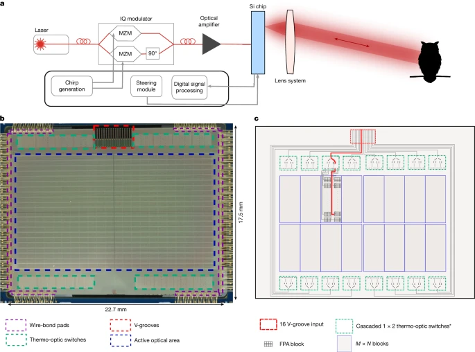
a, The architecture contains an imaging chip that simultaneously functions as both transmitter and receiver. The light path from the chip to target (owl) is determined by the optical lens system. b, Microscope image of the chip, showing the active optical area and thermo-optical switching network. c, Schematic of the light path selection process on the imaging chip. *Some of the outputs of the first-level switches are not connected.
Moreover, the use of coherent detection makes the system immune to possible external interferences and reduces the optical power requirements, as only scattered light that is coherent with the LO and propagating in the matching optical mode as the outbound light is detected.
The FPA presents 16 optical fibre inputs that enable multichannel operation. Each fibre is coupled to an independent switch tree, which feeds a portion of the array. The first stage of the switch network, located outside the pixel array, comprises five layers of 1:2 thermo-optic switches, creating a 1:32 switching structure, which steers light to selected blocks of coherent pixels, as shown in Fig. 1c. A schematic representation of a block of the FPA is presented in Fig. 2a. Within each block, a second stage of the switch tree redirects the light into one of 16 pixel rows. This configuration ensures that each of the 16 fibre inputs can be guided to 32 × 16 possible positions through the two-stage switching hierarchy. In the first stage, 484 outputs out of the possible 512 are routed to the FPA blocks, with the remaining positions left unconnected. Together with the second-stage 1:16 switches, embedded in each FPA block, 7,744 8-pixel rows are enabled.
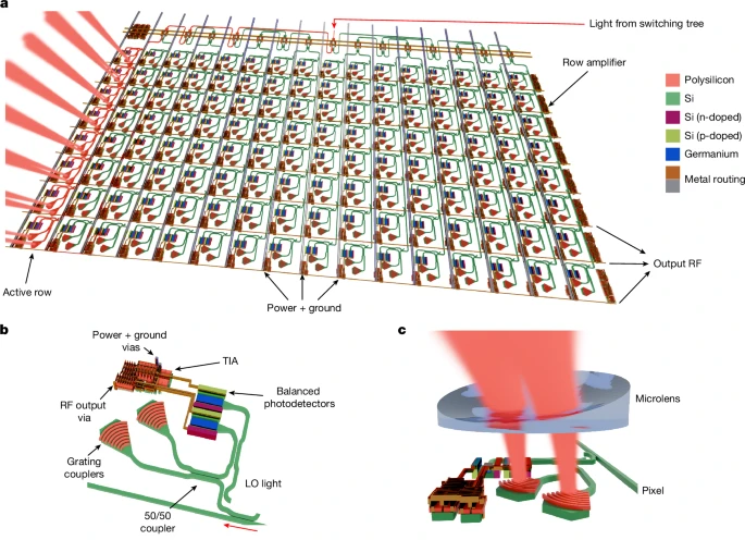
a, Schematic representation of the coherent FPA block. The modulated light is routed to a single 8-pixel row, illuminating a subsection of the scene. The in-plane rotation and emission angle of each grating coupler pair are adjusted to enhance detection efficiency. b, Schematic image of a single coherent pixel, including grating coupler pairs, balanced germanium photodetectors and an integrated TIA. c, Schematic image of a single element of the concave microlens array deposited on-chip to increase light-coupling efficiency.
The calibration of the entire switching tree is performed using monitor photodiodes integrated at the end of each stage.
Each row contains a passive 1:8 optical splitter that distributes the frequency-modulated light equally to individual pixels, allowing all gratings in the 8-pixel row to transmit and receive in parallel. The pixels are placed at a pitch of 53 μm in both directions in the block as in Fig. 2a. This modular pixel/switch block design enhances scalability, enabling an array size of 352 × 176 pixels. Each fibre input can illuminate a different row of 8 pixels simultaneously, allowing 128 pixels in total to be illuminated at any one time.
Within the single-coherent-pixel architecture, the same grating couplers transmitting the modulated light also collect the scattered light from the target. As illustrated in Fig. 2b, the LO light is mixed with the backscattered light collected from the target through a 50/50 directional coupler, generating a heterodyne tone on balanced germanium PIN photodetectors located within each pixel. This detection configuration is referred to as monostatic and it inherently prevents optical cross-coupling between pixels. Only one imaging lens is needed and, unlike in the bistatic configuration13, no alignment of the inbound and outbound optical paths is required. The light-coupling efficiency to and from the target has been optimized by varying the out-of-plane emission angle and in-plane rotation of the grating coupler pairs for each pixel12. Owing to the absence of a compact integrated circulator, a directional coupler and two grating couplers per pixel are used to maximize output power. A further enhancement in collection efficiency is achieved by the deposition of a custom-designed concave microlens directly on-chip, as sketched in Fig. 2c (Methods and Extended Data Figs. 1 and 2).
The balanced photodiode pair present in each pixel rejects common-mode noise. The photocurrent difference containing the beat frequency tone is amplified by a pixel-integrated transimpedance amplifier (TIA)29. Further amplification is used to drive the long lines to the pad drivers at the edge of the FPA. Here the signals are multiplexed, converted to differential signals and driven off-chip. The output signals are externally digitized using analogue-to-digital converters (ADCs) and processed to extract the target distance, velocity and amplitude for each pixel.
Integrated control electronics achieve overall steering by sequentially activating each pixel row in a single FPA block before steering to the next one. High frame rates of 15 fps can be achieved when using approximately 130 μs pixel readout time and the 128 electrical outputs of the sensor simultaneously read and processed. Alternatively, fewer channels could be read in parallel and a lower frame rate achieved.
System performance
The performance of the presented coherent 4D imaging system is demonstrated in Fig. 3. Here we use commercial, non-optimized short-wave infrared (SWIR) lenses to image both static and dynamic scenes. In Fig. 3a, distance information for each pixel is extracted from a single up–down chirp of 32 μs each. To capture the whole scene shown in Fig. 3d with eight parallel readout channels takes one second, or a frame rate of 1 fps. With full parallelization of the readout, a 15 fps frame rate is possible (see Methods section ‘Data acquisition and signal processing’). This highlights the capability of the system for real-time 4D imaging using as little as 11 nJ of energy per point.
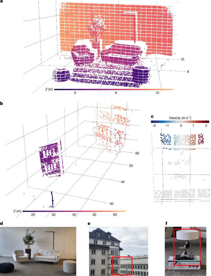
a, Point cloud of an office scene (6–11 m) obtained by a single acquisition using the entire imaging array with a f = 35 mm focal length lens. b, Point cloud from two buildings located 20–65 m away, obtained by coherently averaging four acquisitions with a f = 50 mm focal length lens. c, Velocity-annotated point cloud of the disc that is rotating about its vertical axis, obtained using a single acquisition with a f = 35 mm focal length lens. d–f, Photographs of the scenes in a–c. Red rectangles denote the regions of interest.
The lens used determines the FOV (see Methods section ‘System imaging properties’). In the office scene example, the selected off-the-shelf lens when combined with the imaging sensor reaches a FOV of 32.6° × 19.3° (H × V) with a minimum angular resolution of 0.06° in both dimensions, as obtained from the point cloud in Fig. 3a. In a FPA, the signal-to-noise ratio (SNR) and the frame rate can be traded off by coherently averaging several chirps31. Figure 3b presents a 3D point cloud of a scene beyond 65 m on estimated 30% reflectivity targets30 outside our offices, as shown in Fig. 3e, using the coherent averaging of four chirps and 46 nJ per point. Notably, despite the use of a non-specialized optical lens, architectural details such as windows and facade features remain resolved. These values reflect the ability of the system to densely sample scenes, even without lens optimization. Figure 3c,f shows the point cloud of the spinning disc at 6 m with its velocity readings visualized and a photograph of the disc, respectively. The gaps in the point clouds arise from small separations in the FPA design, specifically the spaces between pixel blocks that are used for electronic and photonic routing.
The SNR for a single-shot measurement depends on several factors, such as transmit power, LO power, beam size and quality, chirp linearity, integration time and laser linewidth. To approach the shot-noise limit, the LO optical power and TIA gain can be appropriately selected so that shot noise dominates over the amplifier thermal noise32,33. The optical power reaching each pixel was measured by monitor photodiodes at the end of each row and adjusted by the measured splitting ratio of the passive splitter. The resulting distribution is shown in Fig. 4a, with a mean of PSP = 426.7 μW. Considering the emission efficiency of the grating couplers and other system losses, this results in an average output power PTX = 178 μW and a mean LO power of PLO = 10.1 μW. The variation over the whole array is within acceptable levels. The amplifier and shot noise were measured for every pixel in the array and the distribution of the ratio is shown in Fig. 4b, with a mean ratio of κ = 0.62. With respect to a pure shot-noise-limited system, this results in a loss of SNR of around 5.6 dB, as presented in Fig. 4c. The shot-noise limit could be achieved by increasing the value of the LO optical power and/or TIA gain to reach a shot-to-amplifier noise magnitude ratio exceeding the value of 2.
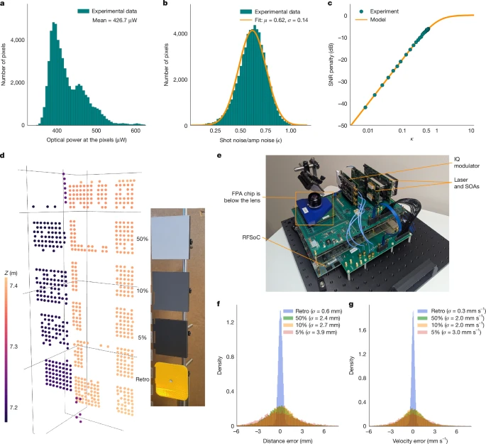
a, Distribution of optical power levels arriving at each pixel, measured by integrated monitor photodiodes. b, Distribution of the measured shot-noise to amplifier-noise magnitude ratio κ over the array. The mean value of κ is 0.62. c, SNR loss as a function of the shot-noise to amplifier-noise ratio. Operating at κ = 0.62 results in a SNR loss of −5.6 dB below a shot-noise-limited system. d, Point cloud obtained with coherent averaging of three frames from the stationary calibrated targets at 7.2 m and photograph of the three calibrated targets with known Lambertian reflectivities and a retroreflector (‘Retro’). e, Photograph of the entire system. SOA, semiconductor optical amplifier. f,g, Distribution of distance (f) and velocity (g) measurement errors.
Furthermore, Fig. 4d shows a variety of stationary targets of calibrated reflectivity placed at 7.2 m, together with the corresponding point cloud, in which no blooming owing to the proximity of a retroreflector to a 5% reflectivity target is noticeable. The distance and velocity precision are quantified on each target as in Fig. 4f,g. The performed analysis is explained in detail in Methods (see Methods section ‘LiDAR measurements’, Extended Data Fig. 5 and Extended Data Table 2). For a target of 5% reflectivity, the standard deviation remains low, with a precision of σ = 3.9 mm and σ = 3.0 mm s−1 for position and velocity, respectively, within most user requirements.
For a specific emitted optical power and integration time, a critical parameter for the system performance is the chosen lens and its ability to provide a collimated beam optimized over the given measurement range of interest. This ensures a constant SNR across the entire measurement range (see Methods section ‘SNR model’). The FOV and angular resolution of the 4D imaging sensor are also determined by the imaging lens, shown in Fig. 4e. Good performance beyond 65 m is achievable with a lens optimized for longer ranges (Methods and Extended Data Figs. 3 and 4).
Conclusion and outlook
In this paper, we have demonstrated a highly scalable, fully integrated 4D imaging FPA sensor, consisting of 352 × 176 pixels, which achieves a radial range of 65 m and an angular resolution of 0.06° with as little as 46 nJ of energy per point and an average of 178 μW of on-target optical power per pixel. With its near QVGA (quarter video graphics array) resolution and more than 0.6 million photonic components, this coherent 4D imaging sensor represents, to our knowledge, the largest coherent FPA produced so far, with five times the number of pixels compared with previous demonstrations12 (Methods and Extended Data Table 1). This brings the sensor resolution within the requirements of most applications. Also, it is the first demonstration of a large-scale coherent FPA with all of the associated electronics integrated on-chip, leading to the cost structure necessary for widespread adoption. Owing to its low emitted optical power and its modular structure with a monostatic pixel design, the presented FPA satisfies the simultaneous stringent requirements across diverse markets, such as eye safety, performance, reliability under real-life conditions and simplicity of module manufacturing. In analogy with a CMOS camera, the system offers high flexibility in range, FOV and angular resolution, as these characteristics are determined by the selected optics.
In the next generation of the FPA, an improvement of the SNR of about 5.6 dB can be achieved by a simple modification of the pixel design, aimed at increasing the LO power to reach the shot-noise-limited regime. Moreover, the performance of the system can be further improved by increasing the optical power transmitted by the pixel. The optical power limitations in silicon owing to nonlinear absorption effects can be overcome through the use of new blended Si–SiN architectures34,35. This would enable a tenfold increase in power delivered to a single pixel, which—in combination with the SNR improvement as a result of LO optimization—could extend the detection range to more than 200 m. Moreover, the second-stage switches embedded at present within the array will be relocated outside the array to enable uniform pixel placement and to eliminate gaps in the far field.
The presented FMCW FPA LiDAR camera-like system offers a compact, low-cost, scalable and adaptable 4D imaging solution, effectively proposing a CMOS camera equivalent for the multidimensional imaging of the world.
Methods
Design and fabrication
Photonic device and circuit-level simulations were performed using ANSYS Lumerical tools, whereas the integrated electronics followed a design flow using Cadence Virtuoso.
The finalized design was verified against the design rules using Cadence’s Physical Verification System (PVS). The demonstrated integrated monostatic FPA was fabricated using GlobalFoundries’ 45SPCLO 300-mm silicon photonics platform, which enables monolithic integration of photonic devices with 45-nm silicon-on-insulator RF CMOS electronics. Most of the photonic devices in the demonstrated FPA were based on the foundry’s standard process development kit but were further miniaturized to meet stringent footprint requirements, allowing the integration of 61,952 pixels. Several dies from different wafers were tested and no inoperative thermo-optic switches or dead pixels were observed; however, a mean of 42 out of 61,952 pixels showed noise greater than twice the mean over the entire array, leading to reduced SNR.
Loss budget
The FPA is supplied with FMCW light through 16 optical channels by means of a fibre ribbon. Each channel passes through a switch network before reaching its designated pixel row. This switch network consists of cascaded 1:2 thermo-optic switches, with the first five switching layers located outside the pixel array and an extra four layers integrated within each pixel block. The switch architecture introduces approximately 0.4 dB of loss per layer outside the array and 0.5 dB per layer within the pixel block, resulting in a total switching loss of around 4 dB. An extra insertion loss around 0.7 dB occurs at the V-grooves36, in which optical fibres are coupled to the chip.
A mean value of 426 μW per pixel is measured when 32 mW is delivered per optical channel. Nonlinear effects such as two-photon absorption and free-carrier absorption37 limit the power in silicon waveguides to approximately 16 mW. The extra 4-dB loss is attributed to a combination of two-photon absorption/free-carrier absorption and routing. Nonlinear losses can be eliminated by the use of advanced architectures combining efficient distribution of power in silicon waveguides with silicon nitride components and efficient routing.
Experimental set-up
The experimental set-up used for the measurement in Fig. 3 is presented in Fig. 4e. Frequency-modulated light at 1,310 nm is generated from a fixed frequency butterfly-packaged single-mode DFB laser (Innolume DFB-1310-PM-50-NL) with a linewidth of approximately 100 kHz. The infrared light from the seed laser is modulated using a silicon photonics IQ modulator. The modulated output then undergoes two-stage amplification using booster optical amplifiers (BOA-1310-50-PM-200mW).
To enable simultaneous operation of different sections of the 4D imaging sensor, the FMCW light is split into 16 fibres and coupled into the FPA through V-groove inputs. To ensure stability and optimal performance, all 16 polarization-maintaining optical fibres required for the full array must be precisely aligned and epoxied into the V-grooves38,39.
The lens systems used for imaging in Fig. 3 are the commercial lenses VS-3514H1-SWIR and VS-5018H1-SWIR from VS Technology with focal lengths f of 35 mm and 50 mm, respectively. They are mechanically attached to the imaging FPA by means of a 3D-printed adaptor, designed to place the lens at the proper working distance. The adaptor is mechanically screwed onto the carrier board. This configuration eliminates relative movements between the imaging FPA and the lens, therefore decreasing the sensitivity of the system to mechanical vibrations.
FPA emission characterization
To characterize the different grating couplers used in the FPA design, the far-field behaviour of dedicated test structures was measured using the knife-edge technique40. The normalized power emitted by a grating designed with a 10° emission angle in the back end of the chip, as a function of the blade position, is presented in Extended Data Fig. 1a. The blade is oriented perpendicular to the propagation direction of the light, as illustrated in Extended Data Fig. 1b.
The Gaussian beam widths at different distances from the chip were extracted by fitting the measurements with the knife-edge formula. The results are presented in Extended Data Fig. 1c for two test structures designed for 7.5° and 10° emission angles. Using the Gaussian beam propagation formula, the estimated beam waists are ω0,7.5° = 2.57 ± 0.01 μm and ω0,10° = 2.48 ± 0.01 μm, respectively. The corresponding half-angle divergences are θ7.5° = 0.165 rad and θ10° = 0.167 rad.
The emission angle and orientation of the grating emitters within the pixels vary depending on their location in the FPA. An orientation distribution similar to that reported in ref. 12 was used to maximize the optical transmission through the imaging lens. On the basis of Lumerical 3D FDTD simulations, the emission angles of the grating couplers were selected to range from 7.5° to 17.5°, increasing progressively with the distance of the emitter from the centre of the FPA. In this analysis, representative 7.5° and 10° gratings couplers were measured.
System imaging properties
The optical properties of the LiDAR system are a convolution of the FPA emission, which can be tuned with the use of a concave microlens deposited on-chip, and the optical lens system. The microlens serves two purposes. As shown in Extended Data Fig. 2a, one microlens per pixel was used to modify the out-of-plane emission angle of the grating couplers, to optimize transmission and FOV over the entire FPA. Simultaneously, the microlens increases the beam divergence of the grating couplers to exploit the entire aperture of the imaging lens. On the basis of Zemax simulations, the emission half-angle divergence of a single grating coupler designed for 7.5° has been increased from θ7.5° = 0.165 rad to θ7.5° = 0.237 rad on average.
The Gaussian-like profile of the emitted beam is shown in Extended Data Fig. 2b for one pixel close to the FPA centre, with (top) and without (bottom) the microlens, for a test imaging lens with f = 25 mm (VS-2514H1-SWIR from VS Technology) in a focusing configuration at around 11–12 m. The emission at the far edge of the lens is affected by aberrations owing to the high angle of incidence of the beam and only partial filling of the lens aperture. For imaging lenses with larger apertures, this phenomenon is strongly reduced.
The Rayleigh range of the 4D imaging system was determined by recording the emitted mode at different distances from the sensor with a SWIR camera (Goldeye G-008 SWIR from Allied Vision). The full width at half maximum of the imaged mode intensity distribution along the x,y axis, perpendicular to the light propagation direction, have been subsequently measured and the average Gaussian beam radius computed according to the formula \(w(z)=\sqrt{\frac{{({w}_{x}(z))}^{2}+{({w}_{y}(z))}^{2}}{2}}\), in which \({w}_{x,y}=\frac{{{\rm{FWHM}}}_{x,y}}{\sqrt{2\mathrm{ln}(2)}}\).
The results of the measurement for the non-collimated imaging configuration are shown in Extended Data Fig. 2c. From the experimental fit for a Gaussian beam propagation, without the microlens, the system presents a Rayleigh range of 5.6 m and a Gaussian beam waist of 1.53 mm at the focal point, placed at 12.5 m from the FPA. The introduction of the microlens allows for a better filling of the lens aperture, leading to a smaller Gaussian beam waist of 1.31 mm at the focal point, placed at 11.1 m from the FPA, and a Rayleigh range of 4.1 m.
For imaging systems used in a collimated configuration, the Rayleigh range of the LiDAR system is determined by the aperture size of the lens, D. Their relation is described by the formula \({z}_{{\rm{R}}}=\frac{{D}^{2}{\rm{\pi }}}{2\lambda }\), in which D = 2ω0 and λ is the wavelength of the emitted light. Therefore, the use of a microlens would lead to a better filling of the aperture of the lens and to a corresponding increase in the Rayleigh range.
According to ray optics, the FOV of the system is related to the focal length f of the lens through the formula12 \({\rm{FOV}}=2{\tan }^{-1}\left(\frac{s}{2f}\right)\), in which s is the chip dimension. The theoretical angular resolution θres of the system is estimated as \({\theta }_{{\rm{res}}}=2{\tan }^{-1}\left(\frac{p}{2f}\right)\) (ref. 12), in which p is the pitch of the pixels.
The influence of the focal length f of the lens on the FOV and angular resolution of the LiDAR system is shown in Extended Data Fig. 3a–c. Point clouds of the same scene have been acquired using three lenses with focal lengths f = 25, 35 and 50 mm. As shown in the figure, the FOV is inversely proportional to the focal length of the lens used, decreasing from an initial value of FOV25mm = 44.44° × 26.65° to FOV50mm = 23.11° × 13.55°. An increase in focal length will also translate into a higher angular resolution of the FPA. The experimental minimum angular resolution was measured as the mean minimum angle between adjacent pixels, excluding the gaps. The measured FOVs and angular resolutions are in good agreement with the theoretical predictions, as summarized in the table reported in Extended Data Fig. 3d.
LiDAR control and electronics
All components of the LiDAR system (laser, IQ modulator, semiconductor optical amplifier, FPA) are mounted on custom-designed carrier boards, which interface by means of a motherboard. System control, chirp generation, signal acquisition and data processing are performed on the AMD Zynq UltraScale+ RFSoC (RF System-On-a-Chip) ZCU111 evaluation board. This integrates processor cores for control, an eight-channel ADC for signal acquisition, a two-channel digital-to-analogue converter (DAC) for chirp generation and programmable logic for digital signal processing.
The chirp for modulation is generated digitally on the field-programmable gate array using direct digital synthesis and the two quadrature signals are generated on the integrated 14-bit 6.5-GSPS DACs. The IQ modulator board amplifies these signals and tunes the modulator arms for single-sideband modulation. The chirp length is 32 μs up, 32 μs down and the total chirp bandwidth is 6 GHz. This sets the system range resolution to 25 mm using ΔR = c/2B (ref. 14).
Each thermo-optic switch arm on the FPA has an unknown phase offset. An automatic calibration routine is run through the RFSoC for the entire switch network. The voltage of each switch arm is swept and embedded photodiodes in the array measure the power at each output. The voltage corresponding to the maximum output is determined and stored by the RFSoC processor. To steer light to a specific position in the array, the prestored calibration values are set by a Serial Peripheral Interface to integrated DACs in the switching array. The switches settle in about 10 μs.
Data acquisition and signal processing
Each of the 16 input channels of the FPA can be illuminated simultaneously, resulting in up to 128 output signals from the chip, which supports a maximum of 20 fps at 100 μs per pixel. For a commercial product, this would require an application-specific integrated circuit to support this high frame rate. Although this is under development, the off-the-shelf RFSoC used at present supports eight acquisition channels. Thus, we acquired 8 pixels simultaneously and multiplexed all of the output channels to read the full array instead of using all 128 signals in parallel. Rows of 8 pixels are read consecutively, stepping through the entire array. The entire step of reading, processing and steering takes 130 μs. This allowed a maximum frame rate of 1 fps with real-time steering, acquisition, processing and data transfer to a PC. Further optimization of the hardware could improve acquisition speed and frame rate.
The output analogue signals are filtered and digitized by the 4,096-MSPS ADCs on the RFSoC. They are then decimated to 256 MSPS. The signals are acquired synchronously to the chirp. On the programmable logic, the samples are multiplied by a window function, a fast Fourier transform with a fixed length of 8,192 samples is performed and the signal magnitude calculated, all in fixed point. If selected, coherent averaging of several chirps is performed. The position of the highest peak is detected on the field-programmable gate array and passed to the processor. The peak frequency is then interpolated and the two chirps are combined into distance, amplitude and velocity. Although the hardware provides the possibility to measure several echoes, the results shown all use the strongest detected echo only. The data are then passed to a PC for display and storage by means of an Ethernet interface. All manually inspected amplitude spectra showed Fourier-limited signals, indicating a sufficiently narrow laser linewidth and sufficient chirp linearity for the measured distances.
Performance comparison
The performance of our 4D imaging system has been compared with a selection of LiDARs presented in the literature. The results are reported in Extended Data Table 1. The comparison includes studies focused on OPAs10,11,19,41,42,43, FPAs12,13,22, fully integrated single-pixel LiDARs16 and transceivers17. The comparison highlights not only system performance metrics such as FOV, maximum range, resolution and energy per pulse or up and down chirps but also focuses on the level of integration of the systems, in particular on the presence of a co-integrated transceiver on-chip as well as monolithic integration of CMOS electronics, including TIAs and photodetectors.
SNR model
A key driver of LiDAR performance is the number of photons received from the target. For a coherent monostatic pixel, the received optical power PRX can be modelled by44:
in which PTX is the transmitted optical power, λ the light wavelength and ω(z) is the Gaussian beam radius of the detecting beam at distance z from the emitter. The total losses of the system are described by the parameter ηp, which includes losses of the lens system, directional couplers and grating couplers. The constant Ï(Ï€) represents the inverse steradian power reflectivity of the target, as defined in ref. 44. The received signal of optical power PRX mixes with the LO of optical power PLO and creates a beat signal with frequency f0 and amplitude given by:
in which RPD is the responsivity of the photodetector.
The recombined optical power in the pixel creates shot noise on each photodetector, which can be modelled as white noise with the noise equivalent bandwidth Be:
An efficient detection of the signal frequency requires the signal peak power spectral density (PSD) to rise above the noise PSD. The SNR is defined experimentally by the ratio of the peak PSD of the target |S(f0)|2 to the mean PSD of noise <|S(fn)|2>. For a shot-noise-limited system, this is given by:
giving the well-known relationship between SNR and the number of detected photons N in the integration time T (ref. 44).
As shown in Fig. 4b, the presented imaging system is not shot-noise limited but contains further noise sources affecting the signal output, including laser frequency noise, TIA thermal noise and ADC noise. Among them, the thermal noise of the amplifier is dominant. Referring the noise sources to the input of the amplifier, the SNR of the imaging system is given by:
in which <Iamp> is the thermal noise of the amplifier. We define the ratio of shot noise to amplifier noise κ using:
The difference between the SNR of the imaging system and its expected SNR in the shot-noise-limited regime defines a SNR penalty as:
We measured the noise ratio κ for each pixel in the array. First, amplifier noise was measured with no light. The mean amplitude in a single bin was measured over 100 acquisitions. Modulated light was then added and the total noise measured in the same way. Shot noise was estimated as \( < {I}_{{\rm{shot}}}^{2} > = < {I}_{{\rm{tot}}}^{2} > - < {I}_{{\rm{amp}}}^{2} > \). The resulting distribution is shown in Fig. 4b, with a mean value of κ = 0.62. As shown in Fig. 4c, this results in a SNR penalty of −5.6 dB.
The dependence of the 4D imaging system’s SNR, as described in equations (5) and (1), on the optical imaging system parameters, particularly the resulting Gaussian beam waist and Rayleigh range, is shown for a single acquisition in Extended Data Fig. 4. The different curves have been obtained for the same optical emitted power PTX characterized in the main text, a single chirp T = 32 μs long and assuming RPD = 0.95 A/W, ηp = 0.23, PLO = 10.1 μW and a 20% reflectivity target. As illustrated, the distance at which the SNR decreases by 3 dB is directly proportional to the emitted Gaussian beam waist. If the beam waist is located at the output of the lens system, the SNR remains approximately constant until the fall-off distance, as shown in Extended Data Fig. 4a. However, for emitted modes with a smaller Gaussian beam waist focused beyond the output aperture of the imaging system, the SNR increases with distance, reaches a maximum at the focal point and then decays rapidly, as shown in Extended Data Fig. 4b. For beams that are well collimated over long distances, no marked change in SNR behaviour is observed over the designed range. In Extended Data Fig. 4c, experimental data acquired on a cardboard target are compared with the theoretical SNR model, computed for a single acquisition using the optical parameters of the 25-mm-focal-length lens shown in Extended Data Fig. 2c. The SNR uncertainty has been computed as the standard deviation over all pixels hitting the target. The data show a good agreement with the theoretical model for a distance up to 17 m from the sensor and a SNR around 1–3 dB larger than expected at longer ranges. This discrepancy could be attributed to the difference between the ideal Gaussian mode modelled and the experimental emitted mode.
LiDAR measurements
Measurements were made with the LiDAR system to determine SNR, detection probability and range precision. Figure 4d shows several stationary targets of calibrated reflectivity placed at 7.2 m. Each target is 10 cm across, corresponding to approximately 100 pixels on each target. To estimate the measurement precision, a LiDAR measurement of the scene was taken 400 times. Noise was measured in a single frequency bin with no target and averaged over all captures. The amplitude of the target signal was measured over all pixels falling on each target, averaged over all captures and scaled by the measured noise figure to give a SNR measurement. False returns giving an incorrect distance measurement were excluded from the calculation to prevent skewing the mean. The results are shown in Extended Data Table 2.
To remove false detections, an amplitude threshold Athresh is defined as four times the mean noise amplitude. Returns with a magnitude lower than this threshold are rejected as invalid points. The detection probability Pdet of a target is measured as the percentage of returns in which the amplitude exceeds the threshold. The false detection probability, Pf, corresponds to the percentage of returns exceeding the amplitude threshold but yielding incorrect distance information outside ±ΔR. The relationship between SNR from different targets and Pdet is shown in Extended Data Fig. 5 and compared with the model \({P}_{{\rm{\det }}}=\exp (-{A}_{{\rm{thresh}}}^{2}/(1+{\rm{SNR}}))\) (ref. 45).
The distance and velocity precision are measured for each pixel on each target. The error of each measurement is calculated by the distance from the mean for each pixel, allowing for slanting of the target. The resulting error distributions of distance and velocity estimations are presented in Fig. 4f,g respectively. As target reflectivity increases, SNR, Pdet and precision all increase.
Data availability
The data used to produce the plots in the main figures of this paper and the extended data figures are available at https://doi.org/10.5061/dryad.6t1g1jxcm. Source data are provided with this paper.
Code availability
The code used to analyse the data, produce the plots in this paper and generate the extended data plots are available at https://doi.org/10.5061/dryad.6t1g1jxcm.
References
Morsy, S., Shaker, A. & El-Rabbany, A. Multispectral LiDAR data for land cover classification of urban areas. Sensors 17, 958 (2017).
Klemas, V. V. Coastal and environmental remote sensing from unmanned aerial vehicles: an overview. J. Coast. Res. 31, 1260–1267 (2015).
Zhang, K., Yan, J. & Chen, S.-C. Automatic construction of building footprints from airborne LIDAR data. IEEE Trans. Geosci. Remote Sens. 44, 2523–2533 (2006).
Mastin, A., Kepner, J. & Fisher, J. Automatic registration of LIDAR and optical images of urban scenes. In Proc. 2009 IEEE Conference on Computer Vision and Pattern Recognition 2639–2646 (IEEE, 2009).
Urmson, C. et al. Autonomous driving in urban environments: Boss and the urban challenge. J. Field Robot. 25, 425–466 (2008).
Luetzenburg, G., Kroon, A. & Bjørk, A. A. Evaluation of the Apple iPhone 12 Pro LiDAR for an application in geosciences. Sci. Rep. 11, 22221 (2021).
Roriz, R., Cabral, J. & Gomes, T. Automotive LiDAR technology: a survey. IEEE Trans. Intell. Transp. Syst. 23, 6282–6297 (2022).
Shekhar, S. et al. Roadmapping the next generation of silicon photonics. Nat. Commun. 15, 751 (2024).
Li, Z. et al. Towards an ultrafast 3D imaging scanning LiDAR system: a review. Photonics Res. 12, 1709–1729 (2024).
Poulton, C. V. et al. Coherent lidar with an 8,192-element optical phased array and driving laser. IEEE J. Sel. Top. Quantum Electron. 28, 1–8 (2022).
Moss, B. R. et al. A 2048-channel, 125μw/ch DAC controlling a 9,216-element optical phased array coherent solid-state lidar. In Proc. 2023 IEEE Symposium on VLSI Technology and Circuits (VLSI Technology and Circuits) 1–2 (IEEE, 2023).
Zhang, X., Kwon, K., Henriksson, J., Luo, J. & Wu, M. C. A large-scale microelectromechanical-systems-based silicon photonics lidar. Nature 603, 253–258 (2022).
Rogers, C. et al. A universal 3D imaging sensor on a silicon photonics platform. Nature 590, 256–261 (2021).
Behroozpour, B., Sandborn, P. A. M., Wu, M. C. & Boser, B. E. Lidar system architectures and circuits. IEEE Commun. Mag. 55, 135–142 (2017).
Lukashchuk, A. et al. Photonic-electronic integrated circuit-based coherent LiDAR engine. Nat. Commun. 15, 3134 (2024).
Sayyah, K. et al. Fully integrated FMCW LiDAR optical engine on a single silicon chip. J. Light. Technol. 40, 2763–2772 (2022).
Martin, A. et al. Photonic integrated circuit-based FMCW coherent LiDAR. J. Light. Technol. 36, 4640–4645 (2018).
Li, C. et al. Monolithic coherent LABS lidar based on an integrated transceiver array. Opt. Lett. 47, 2907–2910 (2022).
Li, Y. et al. Wide-steering-angle high-resolution optical phased array. Photonics Res. 9, 2511–2518 (2021).
Pierrottet, D. F. et al. Linear FMCW laser radar for precision range and vector velocity measurements. MRS Online Proc. Library 1076, 10760406 (2008).
Yu, L. et al. Focal plane array chip with integrated transmit antenna and receive array for LiDAR. J. Light. Technol. 42, 3642–3651 (2024).
Inoue, D. et al. Solid-state optical scanning device using a beam combiner and switch array. Optica 10, 1358–1365 (2023).
Na, Q. et al. Optical frequency shifted FMCW Lidar system for unambiguous measurement of distance and velocity. Opt. Lasers Eng. 164, 107523 (2023).
Shi, P. et al. Optical FMCW signal generation using a silicon dual-parallel Mach-Zehnder modulator. IEEE Photonics Technol. Lett. 33, 301–304 (2021).
Xu, Z., Tang, L., Zhang, H. & Pan, S. Simultaneous real-time ranging and velocimetry via a dual-sideband chirped lidar. IEEE Photonics Technol. Lett. 29, 2254–2257 (2017).
Chung, S., Abediasl, H. & Hashemi, H. A monolithically integrated large-scale optical phased array in silicon-on-insulator CMOS. IEEE J. Solid-State Circuits 53, 275–296 (2018).
Abediasl, H. & Hashemi, H. Monolithic optical phased-array transceiver in a standard SOI CMOS process. Opt. Express 23, 6509–6519 (2015).
Kim, T. et al. A single-chip optical phased array in a wafer-scale silicon photonics/CMOS 3D-integration platform. IEEE J. Solid-State Circuits 54, 3061–3074 (2019).
Bhargava, P. et al. Fully integrated coherent LiDAR in 3D-integrated silicon photonics/65nm CMOS. In Proc. 2019 Symposium on VLSI Circuits C262–C263 (IEEE, 2019).
Ilehag, R., Schenk, A., Huang, Y. & Hinz, S. KLUM: an urban VNIR and SWIR spectral library consisting of building materials. Remote Sens. 11, 2149 (2019).
Baumann, B. et al. Signal averaging improves signal-to-noise in OCT images: but which approach works best, and when? Biomed. Opt. Express 10, 5755–5775 (2019).
Collett, M., Loudon, R. & Gardiner, C. W. Quantum theory of optical homodyne and heterodyne detection. J. Mod. Opt. 34, 881–902 (1987).
Rubin, M. A. & Kaushik, S. Squeezing the local oscillator does not improve signal-to-noise ratio in heterodyne laser radar. Opt. Lett. 32, 1369–1371 (2007).
Bian, Y. et al. High-power, low-loss, fabrication tolerant multi-tip SiN edge coupler in 300mm monolithic SiPh foundry technology. In Proc. Optical Fiber Communication Conference (OFC) 2025, M4J.6 (Optica Publishing Group, 2025).
Chandran, S. et al. High performance silicon nitride passive optical components on monolithic silicon photonics platform. In Proc. Optical Fiber Communication Conference (OFC) 2024, Th3H.4 (Optica Publishing Group, 2024).
Giewont, K. et al. 300-mm monolithic silicon photonics foundry technology. IEEE J. Sel. Top. Quantum Electron. 25, 1–11 (2019).
Tokushima, M., Ushida, J. & Nakamura, T. Nonlinear loss characterization of continuous wave guiding in silicon wire waveguides. Appl. Phys. Express 14, 122008 (2021).
Barwicz, T. et al. Automated, self-aligned assembly of 12 fibers per nanophotonic chip with standard microelectronics assembly tooling. In Proc. 2015 IEEE 65th Electronic Components and Technology Conference (ECTC), 775–782 (IEEE, 2015).
Barwicz, T. et al. A novel approach to photonic packaging leveraging existing high-throughput microelectronic facilities. IEEE J. Sel. Top. Quantum Electron. 22, 455–466 (2016).
de Araújo, M. A., Silva, R., de Lima, E., Pereira, D. P. & de Oliveira, P. C. Measurement of Gaussian laser beam radius using the knife-edge technique: improvement on data analysis. Appl. Opt. 48, 393–396 (2009).
Chen, J. et al. Single soliton microcomb combined with optical phased array for parallel FMCW LiDAR. Nat. Commun. 16, 1056 (2025).
Lee, J. et al. Real-time LIDAR imaging by solid-state single chip beam scanner. Electron. Imaging 34, 1–4 (2022).
Jang, B. et al. Real-time imaging of mid-range lidar using single-chip beam scanner. In Proc. Conference on Lasers and Electro-Optics (CLEO): Applications and Technology 2022, ATh2L.6 (Optica Publishing Group, 2022).
Osche, G. R. Optical Detection Theory for Laser Applications (Wiley, 2002).
Piggott, A. Y., Jiang, C. Y., Lam, J., Gassend, B. & Verghese, S. Coherent lidar for ride-hailing autonomous vehicles. In Proc. High-Power Diode Laser Technology XXIII 142–161 (SPIE, 2025).
Acknowledgements
We thank Ö. Cogal for his contributions to digital and software design on the RFSoC, alongside discussions on real-time digital signal processing implementation. We thank G. Reed, D. Thomson and their team at the Optoelectronics Research Centre (ORC) at Southampton University for fruitful discussions. We thank O. von Hofsten from Eclipse Optics for his contribution to free space emission modelling and microlens design. We thank A. Latulippe, W. DiPippo, J. Van Ven Roy and the Holographix team for the microlens manufacturing. We thank V. Gupta, R. Sirdeshmukh, K. Dezfulian, T. Miller and the GlobalFoundries team for the assistance in device fabrication.
Author information
Authors and Affiliations
Contributions
F.F.S., A.C.G., S.A.F. and A.F. contributed equally to the generation of the manuscript. A.F. and F.F.S. built and tested the free space portion of the LiDAR. A.D. designed the external electronic circuits and boards for the LiDAR system. A.D., A.F. P.P., S.A.F. and N.D. wrote the LiDAR system software and firmware on the PC and board microcontroller units. A.D. and P.P. designed and implemented the chirp generation, data acquisition and signal processing chain on the RFSoC. A.F., S.A.F. and P.P. performed the measurements and corresponding modelling. A.C.G., M.S., F.F.S., A.F. and N.D. designed and simulated the custom photonic components of the chip, which were tested by F.F.S. and A.F. M.W. performed validations of the custom-designed components. A.C.G. and M.S. designed and laid out pixels, switch networks, photonic routing and the rest of the photonic integrated circuits. I.E.O. designed and laid out the integrated electronic circuits of the FPA and performed their verification with T.C., P.P. and Y.P. A.C.G., A.F. and M.S. combined the photonic and electronic layouts, performed verifications and prepared the chip for the tape-out. R.N. supervised the project.
Corresponding author
Ethics declarations
Competing interests
All authors are shareholders of Pointcloud Inc., a company specialized in the design of custom LiDAR systems based on FMCW coherent FPAs.
Peer review
Peer review information
Nature thanks Hongyan Fu, Qingyang Zhu and the other, anonymous, reviewer(s) for their contribution to the peer review of this work. Peer reviewer reports are available.
Additional information
Publisher’s note Springer Nature remains neutral with regard to jurisdictional claims in published maps and institutional affiliations.
Extended data figures and tables
Extended Data Fig. 1 Chip emission characterization.
a, Knife-edge measurement of a single grating with 10° emission angle as a function of distance from the back end. The shift in the centre position of the curves is because of the non-vertical propagation of the emission. b, Schematic representation of the knife-edge measurement set-up configuration. c, Beam divergence for grating couplers with 7.5° (blue) and 10° (green) emission angles and their respective Gaussian fits (red). Here the error bars represent the measurement resolution of the blade positions.
Extended Data Fig. 2 Microlens emission characterization.
a, Out-of-plane emission angle correction in absolute value introduced by the microlens. The final out-of-plane emission angles result decreased from around 4–7° at the centre of the chip and up to 11° at the far corners of the FPA. b, Image of the emitted Gaussian beam near the focal point without (bottom) and with (top) the microlens. c, Measured average Gaussian beam waist and fitted Gaussian beam propagation function (dotted line) as a function of distance from the sensor for the system with (green) and without (blue) the microlens for a lens with f = 25 mm. The error bars represent the measurement uncertainty of the camera position.
Extended Data Fig. 3 Point clouds of the same office scene obtained using different lenses.
a–c, 25 mm (a), 35 mm (b) and 50 mm (c) focal lengths. Each point cloud is the result of three coherently averaged acquisitions. d, A table comparing the FOV and minimum angular resolutions of the lenses used with the theoretical values.
Extended Data Fig. 4 SNR model.
a,b, Simulated values of the SNR from our 4D imaging system using different lenses. The results are shown for emitted modes with a Gaussian beam waist from ω0 = 0.5 mm to ω0 = 5 mm, with their maximum focusing point situated at the lens output aperture (a) or at a distance of 11 m from the lens system (b). The dash-dotted line in b represents the distance from the FPA at which the sensor exhibits −3 dB SNR with respect to the baseline for a Gaussian mode of beam waist ω0 = 1.3 mm, corresponding to 27.1 m. c, Comparison of the theoretical model with experimental data measured on cardboard at different distances. The error bars represent the standard error.
Extended Data Fig. 5 The measured detection probability as a function of SNR for selected calibrated targets.
Obtained by coherently averaging different numbers of acquisitions. The solid line denotes the model in which Athresh is defined as four times the mean noise amplitude.
Supplementary information
Source data
Rights and permissions
Open Access This article is licensed under a Creative Commons Attribution-NonCommercial-NoDerivatives 4.0 International License, which permits any non-commercial use, sharing, distribution and reproduction in any medium or format, as long as you give appropriate credit to the original author(s) and the source, provide a link to the Creative Commons licence, and indicate if you modified the licensed material. You do not have permission under this licence to share adapted material derived from this article or parts of it. The images or other third party material in this article are included in the article’s Creative Commons licence, unless indicated otherwise in a credit line to the material. If material is not included in the article’s Creative Commons licence and your intended use is not permitted by statutory regulation or exceeds the permitted use, you will need to obtain permission directly from the copyright holder. To view a copy of this licence, visit http://creativecommons.org/licenses/by-nc-nd/4.0/.
About this article

Cite this article
Settembrini, F.F., Gungor, A.C., Forrer, A. et al. A large-scale coherent 4D imaging sensor. Nature 651, 364–370 (2026). https://doi.org/10.1038/s41586-026-10183-6
Received:
Accepted:
Published:
Version of record:
Issue date:
DOI: https://doi.org/10.1038/s41586-026-10183-6
